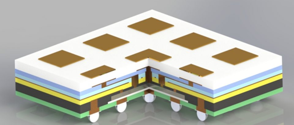
Development of packaging technology at sub-terahertz frequencies (Sub-THz-package)
Sub-terahertz frequencies are being embraced by the upcoming 6G providers as a vehicle to overcome the spectrum crunch in current communications and enable a new era of massively connected devices. Moreover, sensing capabilities will be an integral part of these 6G technologies, thanks to the higher accuracy sensing achieved on radar-like technology arises. For this new 6G technology, new spectral bands are being investigated such as G-band (140-170GHz) and H-band (220-325GHZ), where there are new IEEE 802.15.3d standards that consider up to 70GHz bandwidth.
The advancement of semiconductor technology reaching higher oscillation frequency (fmax) in the terahertz range, has allowed the spread of transmitters and receivers at the sub-terahertz bands (>100GHz) band, using CMOS, SiGe, InP, GaAs... At these frequencies, the packaging strategy is crucial due to the limited SNR obtained with these circuits. It is quite common to see antenna on-package integration at these frequencies since the physical size of antennas is still relatively large and therefore costly to manufacture within the same circuit. Moreover, there is still the need to combine multiple-chip technologies within the same package. All in all, realizing a multi-chip package at sub-terahertz frequencies (>100GHz) that can provide seamless integration with the antenna with low loss and takes into account other aspects such as the thermals and cost, remains a challenge.
This project is in collaboration with Chip Integration Technology Center (CITC) for the development of advanced front-end packaging solutions for the next generation of communications and sensing applications at sub-terahertz frequencies.

Project data
| Researchers: | Maria Alonso-delPino, Cesare Tadolini |
|---|---|
| Starting date: | March 2024 |
| Closing date: | March 2028 |
| Funding: | 300 kE; related to group 300 kE |
| Sponsor: | CITC |
| Partners: | CITC |
| Contact: | Maria Alonso-delPino |